
")
Additive manufacturing
- Written by José Manuel Fernández
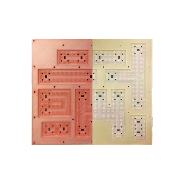
3D printed gap waveguide prototypes before metallization (left) and postmetallization in copper (10 microns) (right)
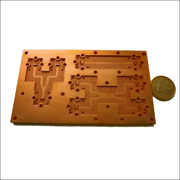
3D printed Butler matrix based on gap waveguide designed at 94 GHz
Full 3D printed Butler Matrix with coupling cavity to the RLSA: Monopulse radar antenna for space debris detection at 94 GHz
Full 3D printed DMLS (Direct Metal Laser Sintering) Butler Matrix with coupling cavity to the RLSA: Monopulse radar antenna for space debris detection at 94 GHz
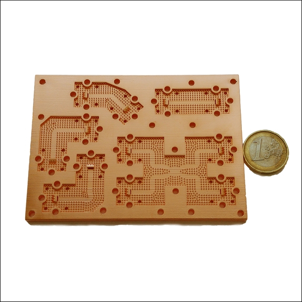
3D printed basic components of the Butler matrix at 94 GHz: right angle bend, 45º bend, short straight section, 90º phase shifter and hybrid coupler
3D printed basic components of the Butler matrix at 94 GHz: power divider, long straight section and crossover
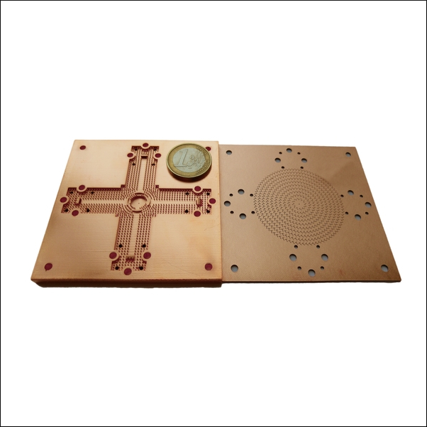
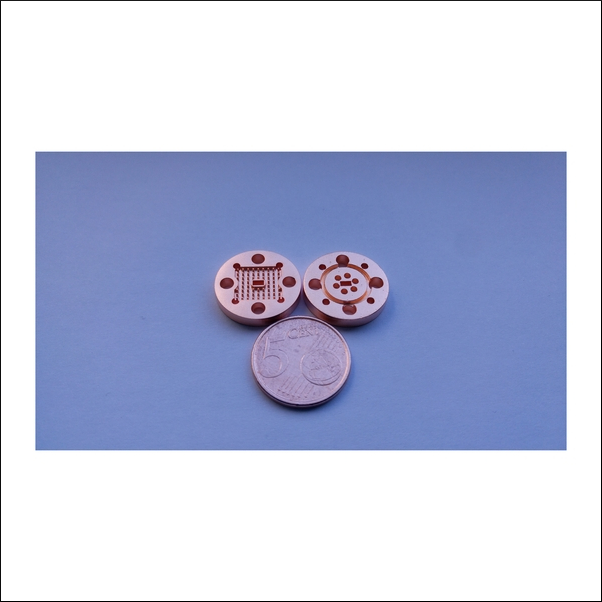
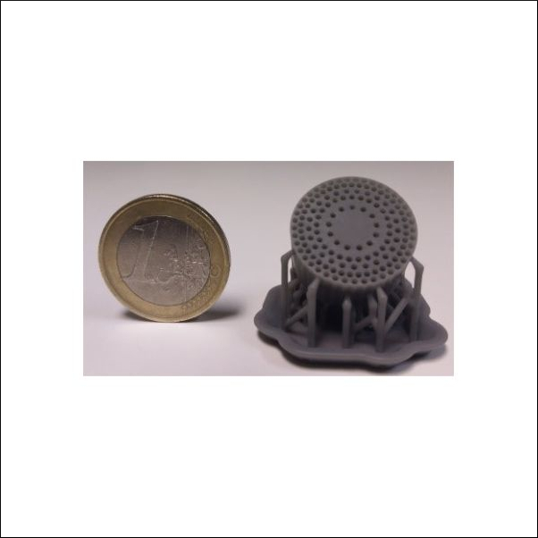
Coupling cavity to the RLSA (Radial Line Slotted Array) printed in 3D
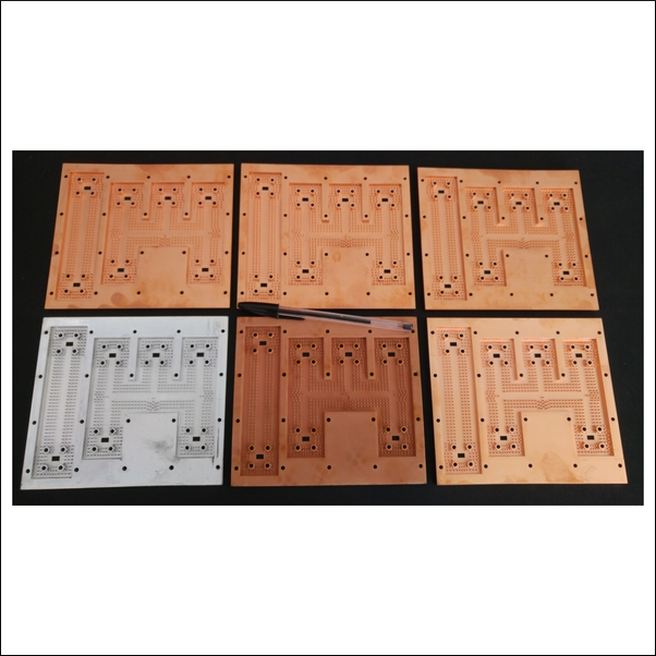
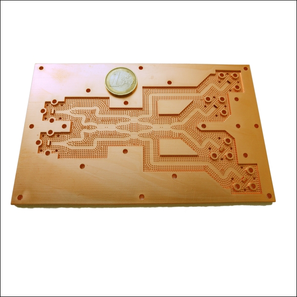
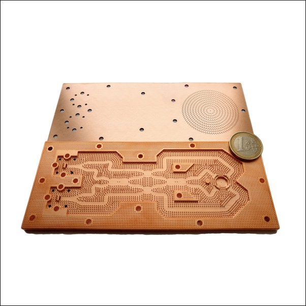
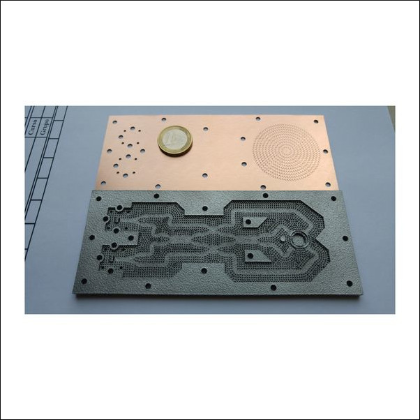
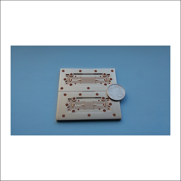
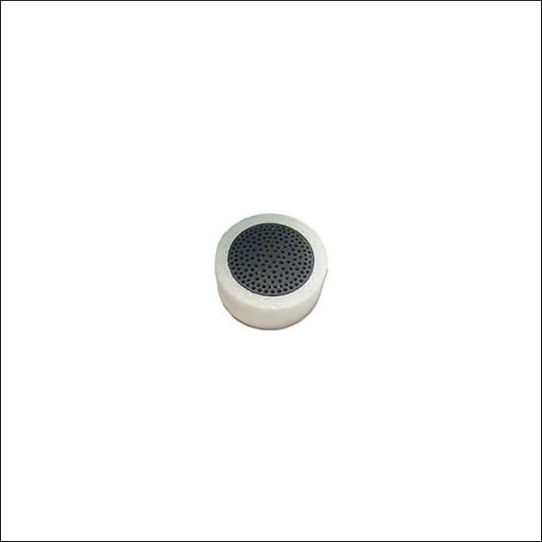
Six 3D printed prototypes manufactured with different materials and metallization techniques
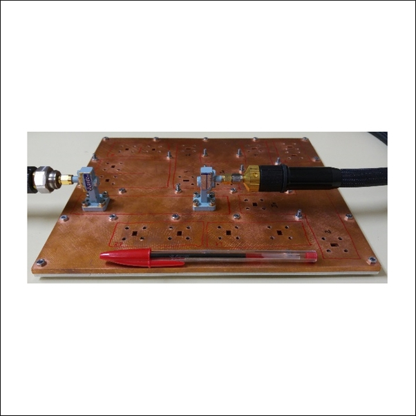
3D printed gap waveguide support structure for an electrically reconfigurable phase shifter based on liquid crystal at W band
3D printed WR-10 flanges with gap waveguide based on pins and circular holes to facilitate the connection of waveguide devices at W band
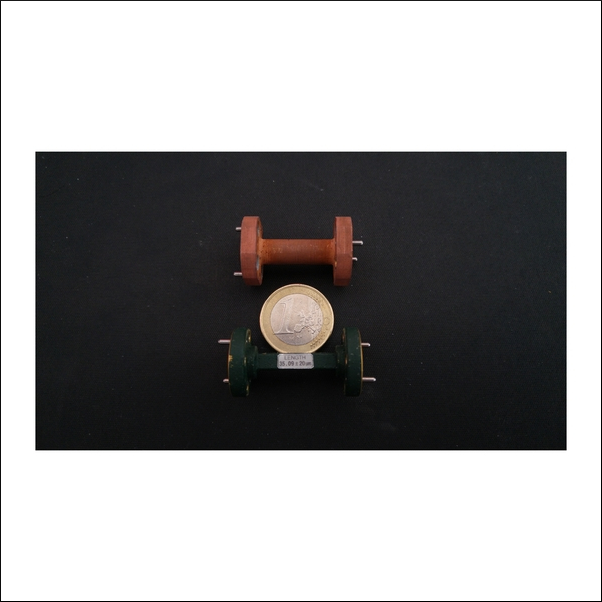
3D printed (top) and commercial machined aluminum (bottom) WR-10 waveguide sections
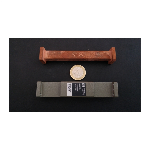
3D printed (top) and commercial machined aluminum (bottom) WR-28 waveguide sections
3D printed waveguide gap prototypes at Ka-band
Perforated 5 layers 3D-Printed Flat Lens for Wideband Millimeter-Wave Applications (45-110 GHz) fabricated with 3D Printer Form 2 from Formlabs
Perforated 5 layers 3D-Printed Flat Lens for Wideband Millimeter-Wave Applications (45-110 GHz) fabricated with 3D Printer Form 2 from Formlabs
Lens integration for Wideband Millimeter-Wave Applications
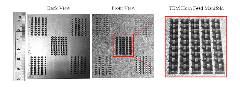
5x9 TEM horn array manifold lens feeder by high resolution DMLS (Direct Metal Laser Sintering) 3D printing in stainless steel for Wideband Millimeter-Wave Applications (45-110 GHz).